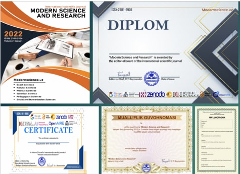
International scientific journal "Modern Science and Research"
ISSN: 2181-3906; OAV Guvohnoma №042359; Impact
factor (UIF-2022): 8.2
Ushbu jurnalda O'zbekiston va chet davlatlar olimlari ilmiy maqolalari
chop etiladi.
Ushbu jurnal OAK ro'yxatida mavjud xalqaro bazalarda indekslanib,
elektron va bosma holatda nashr etib boriladi.
Jurnalning rasmiy tillari: o‘zbek, rus, ingliz
Jurnal telegram kanali: https://t.me/modernscience_research
Maqola muallifiga BEPUL qabul qilinganlik haqida tabriknoma,
sertifikat, indekslanganligi haqida ma'lumotnoma va mualliflik
guvohnomasi beriladi.
Jurnal har oyda nashr qilinadi.
Maqolalar yuborish uchun:
@modernscience_research
golibboymurodov6@gmail.com